

 Phoenix 24
Microscopic pixels could transform sensing, imaging and optical computing.
Cambridge | July 2026
Researchers at the Massachusetts Institute of Technology have developed a chip-based optical device capable of controlling mid-infrared light through microscopic pixels that operate independently. Infobae reported that the technology functions as a programmable metasurface, allowing it to selectively manipulate radiation that cannot be seen by the human eye. The development could eventually support smaller and more precise systems for detecting gases, monitoring pollution, identifying heat losses and producing thermal images.
Mid-infrared light carries valuable information because many chemical compounds absorb specific wavelengths within this region of the electromagnetic spectrum. Methane, propane and numerous organic molecules leave distinctive optical signatures that can reveal their presence even when they are invisible to conventional cameras. Detecting those patterns currently requires specialized systems that can be expensive, large and mechanically complex.
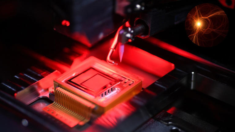
The MIT device approaches the problem by replacing traditional optical components with a thin surface covered by structures smaller than the width of a human hair. These engineered structures form a metasurface capable of changing how incoming light is transmitted. Instead of relying on moving lenses, rotating filters or bulky instruments, the chip modifies its optical behavior electronically.
The central advance lies in the independent control of each microscopic pixel. Earlier tunable metasurfaces could change the focus or optical response of an entire surface simultaneously, but they could not easily adjust individual regions without adding an impractical number of electrical connections. The new architecture allows selected pixels to switch while neighbouring areas remain unchanged.
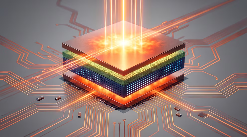
Researchers achieved this control using an arrangement inspired by the wiring systems found in electronic displays and memory technologies. Two layers of conductive lines cross one another at right angles, creating a grid of individually addressable points. At each intersection, an electrical signal activates a microscopic heater positioned beneath the optical material.
The heat changes the atomic organization of a phase-change material integrated into the metasurface. It can alternate between crystalline and amorphous states, each interacting differently with infrared light. By controlling which pixels change state, the device can create programmable patterns across its surface and determine which parts of the incoming radiation are transmitted.
A silicon diode selector was also incorporated into every pixel. This component prevents unwanted electrical currents from reaching adjacent areas and accidentally changing their optical state. Suppressing these unintended pathways is essential if the system is eventually expanded from a small laboratory prototype into a dense array containing thousands or millions of pixels.

The experimental device used a six-by-six matrix containing 36 independently controlled metasurface pixels. Researchers demonstrated that the pixels could be repeatedly activated and deactivated while maintaining reliable performance. Although the array remains small, its purpose was to validate the architecture rather than produce a commercial imaging system.
The design was manufactured using established semiconductor processes and equipment available through MIT.nano and a specialized chip foundry. This compatibility is strategically important because promising laboratory devices often fail to reach industrial production when they require exotic materials or manufacturing methods. A system aligned with conventional chip fabrication has a clearer route toward larger arrays, standardized production and integration with electronic hardware.
Potential applications extend across environmental monitoring, infrastructure maintenance and industrial safety. A compact sensor could be configured to search for the infrared signature of methane escaping from pipelines or propane accumulating near equipment. Similar technology could help identify chemical compounds in the atmosphere and provide more detailed information about pollution sources.
Thermal imaging represents another important possibility. Every object emits infrared radiation according to its temperature, allowing specialized cameras to reveal heat patterns that ordinary visible-light systems cannot capture. Programmable control could help a future camera emphasize particular temperature ranges or extract selected characteristics from a complex scene.
Buildings could also be examined for energy loss through walls, windows and insulation. Industrial operators might detect overheated components before they fail, while emergency teams could search for people in darkness or smoke. Aerospace instruments could use the technology to observe atmospheric compounds or collect more specific infrared information from distant environments.
Military and security applications are also technically possible, particularly in night vision, surveillance and target identification. The research received partial support from United States defense-related programmes alongside scientific institutions. However, the same underlying capability can serve civilian purposes whenever identifying heat or chemical signatures is valuable.
The chip may eventually contribute to a different form of information processing known as optical computing. Conventional processors manipulate electrical signals, while photonic systems use light to transport or calculate information. Metasurfaces can potentially encode parameters used by artificial intelligence models and perform parts of a computational operation as light passes through them.

Such applications remain more distant than chemical sensing or thermal imaging. The present prototype does not constitute a complete infrared camera, artificial intelligence processor or commercial detector. Researchers must increase the number of pixels, improve durability and determine how the device will interact with sensors, control electronics and software.
Scaling will require precise manufacturing because every microscopic heater, diode and optical structure must behave consistently. A defect that affects only a small number of elements in a 36-pixel prototype could become a major reliability problem in an array containing millions. Long-term performance will also depend on whether the phase-change material can complete many thousands of switching cycles without degrading.
The research nevertheless establishes an important foundation. It shows that two-dimensional pixel-level control of a transmissive mid-infrared metasurface can be achieved without connecting a separate wire to every optical element. That architectural solution may be as consequential as the optical material itself because scalability determines whether a scientific demonstration can become practical technology.

The device changes the role of an infrared lens from a passive component into a configurable information filter. Instead of collecting every available signal and processing it later, a future system could be programmed to emphasize the specific features it has been asked to find. Light would not merely enter the camera; it would be organized according to the purpose of the observation.
MIT’s prototype remains an early-stage platform, but its implications reach beyond a single chip. By teaching microscopic pixels to control invisible light independently, researchers are moving toward optical systems that can observe, filter and potentially calculate information before conventional electronics begin processing it.
Phoenix24 | Invisible light, measurable intelligence. Luz invisible, inteligencia medible.